
| Image | Comment |
|---|---|
|
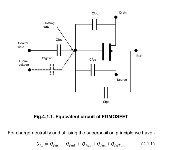
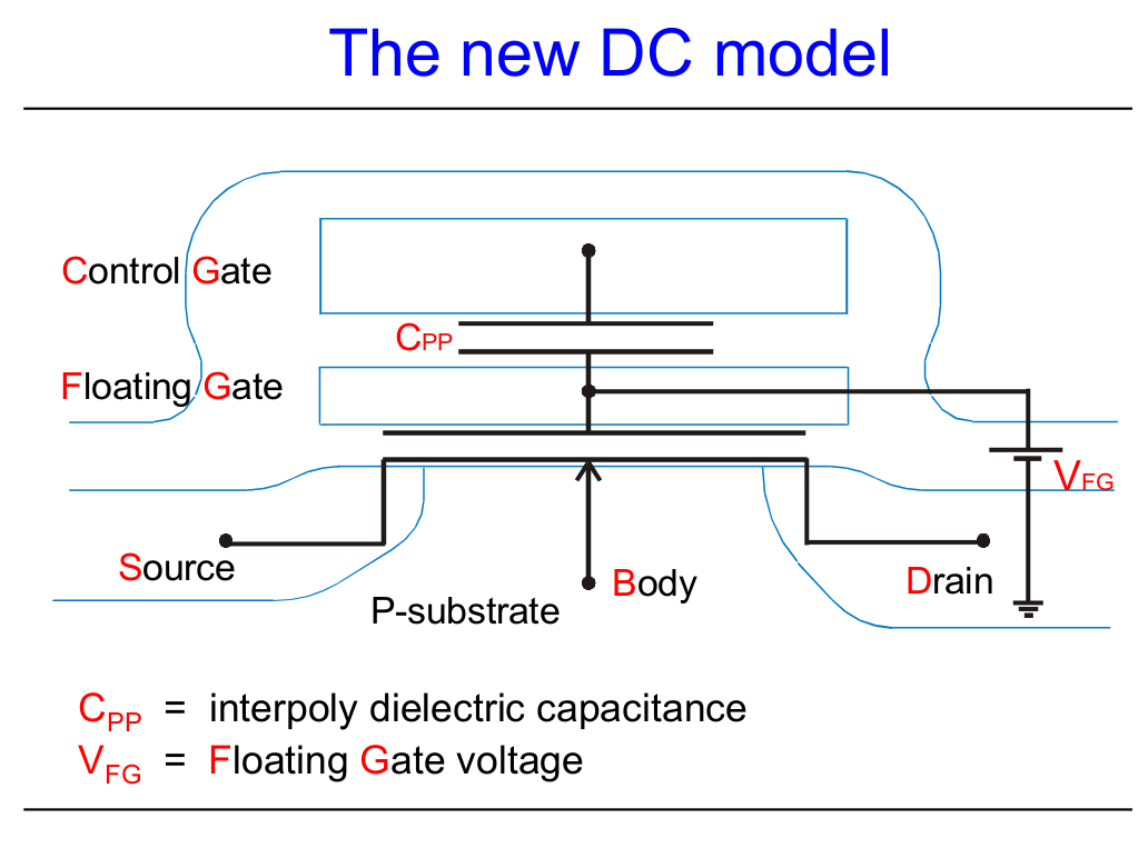
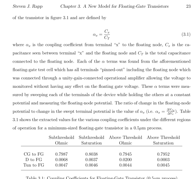
Part 1 page 34 Fig 4.1.1 Eqn 4.1.1. Note the capicator indexing and the charge neutrality equation Eqn 4.1.1. |
|
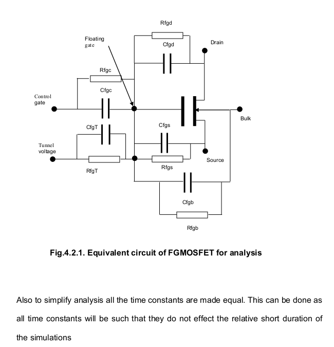
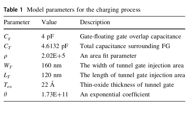
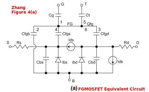
Part 1 page 36 Fig 4.2.1. Using the C=Q/V relationship Fig 4.2.1 is presented as the Equivalent circuit of a FGMOSFET. A shewd constraint is set on all time constants as being equal and large. This removes a level of complexity from the analysis if the "simulations runs" are required to be of relatively short in duration. Note the isolation of the Floating Gate node near the center of the image |
|
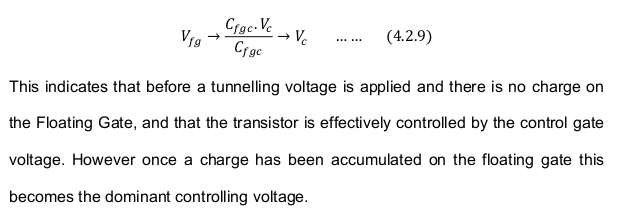
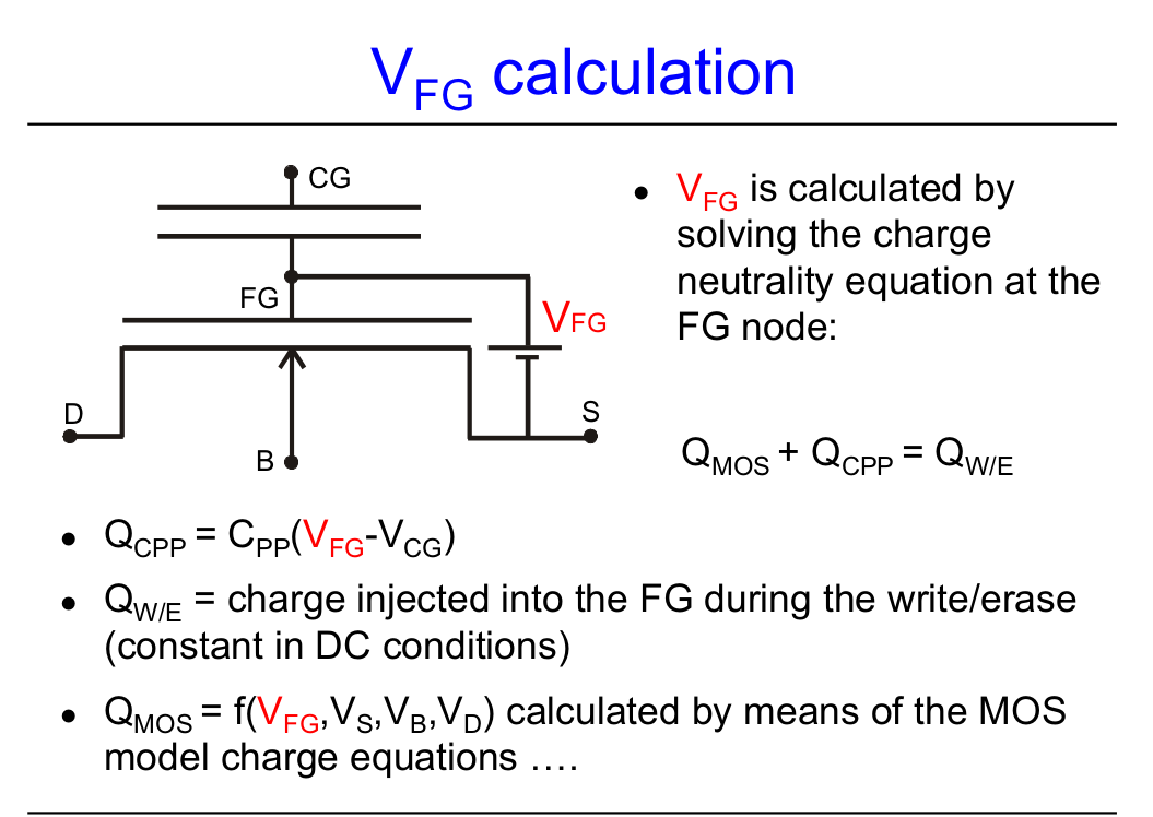
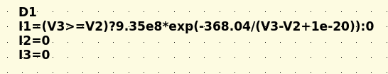
Part 1 page 38 Eqn 4.2.9. For the DC or Steady State operationa mode, following a stepwise set of redefinfitons and assumptions Eqn 4.2.9 was derviced. This equation depicts the direct relationship between the Control Gate voltage and the Floating Gate. This condition exist even though no direct measurement of the floating gate is possible. |
|
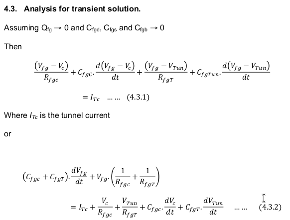
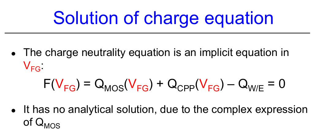
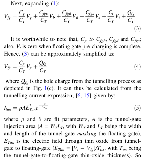
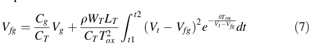
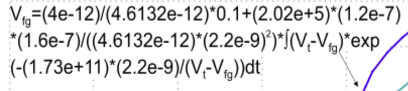
Part 1 page 38 Eqn 4.3.2. The complex nature of Floating Gate Voltage, Eqn 4.3.2, precludes an analytical solution at this time. However, it is
demonstrated within the thesis that a suitable Equation Derived Design can be developed to provide a 'close' approximation
of a FGMOSFET Transient Solution. For charging the model incorporates the Fowler-Nordheim localized current density,
i.e. electron tunneling for charging or charge. This event is often termed programming.
The corresponding compliment, discharing or discharge, is mentioned in the thesis as Channel Hot Electrons. The third term usually associated with charge/discharge of MOSFET memory devices is 'read'. The 'read' is not speciifcally mentioned in the thesis. But like discharge, 'read' will be addressed as we move from a basic cell to more complex Floating Gate device organization. |
|
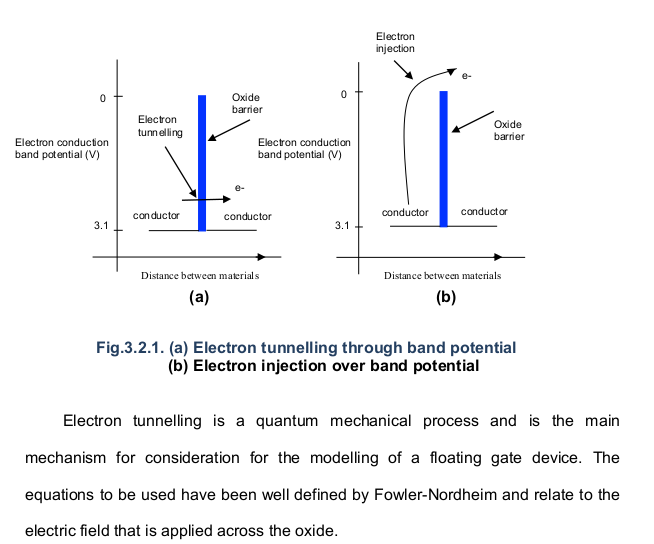
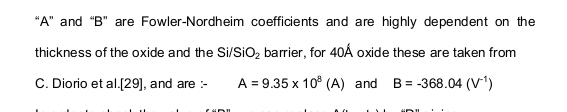
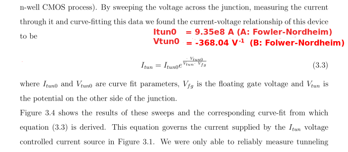
Part 1 page 28 The Fowler-Nordheim appoximation employs two constants that evolve from 'testing' specific MOSFET device 'featrue' physical characteristics. |

|
Merged from Part 1 page 29 Eqn 3.2.1 and page 30 Eqn 3.3.1. Equation 3.3.1 and its derivation form the heart of the thesis
and the cell level anlysis/simulation of this project.
|

|
Part 1 page 42..43 Fig 5.1.1(a) and (b) were replicated using 'qucs' to serve as a shke-down curise for the FGMOSFET model and the test schematic. Variations were found. But the model employed was slightly different. The imprtant verification involved the linear and satuttion regions expected charactertics of the FGMOSFET. |
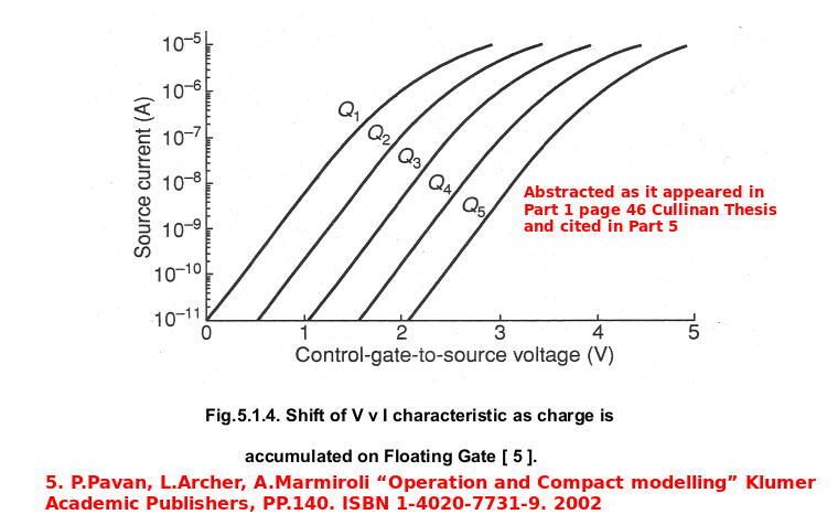
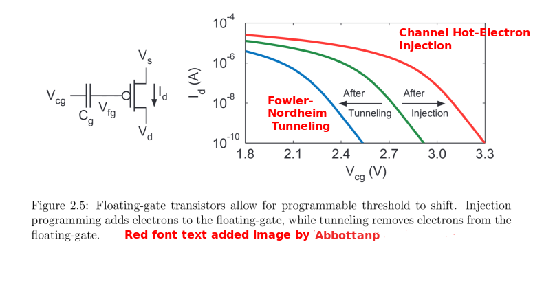
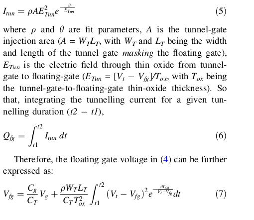
| No Image Used | Ibid. In Part 1 Chapter 5 page 46 of Cullinan thesis employs a reference used in Cullinan's thesis to the Shift in V-I characteristics as charge accumulates on the Floating Gate appears as it was abracted in the Pavan Team Presentation given further below on this webpage. |
|
|
Ibid. Beginning in Part 3 page 52 Cullinan begins to fill the QUCS toolbox with increasingly complex examples of usage of QUCS function and library of devices. This is the part of Cullinan thesis where one needs to return when questions arise. |
|
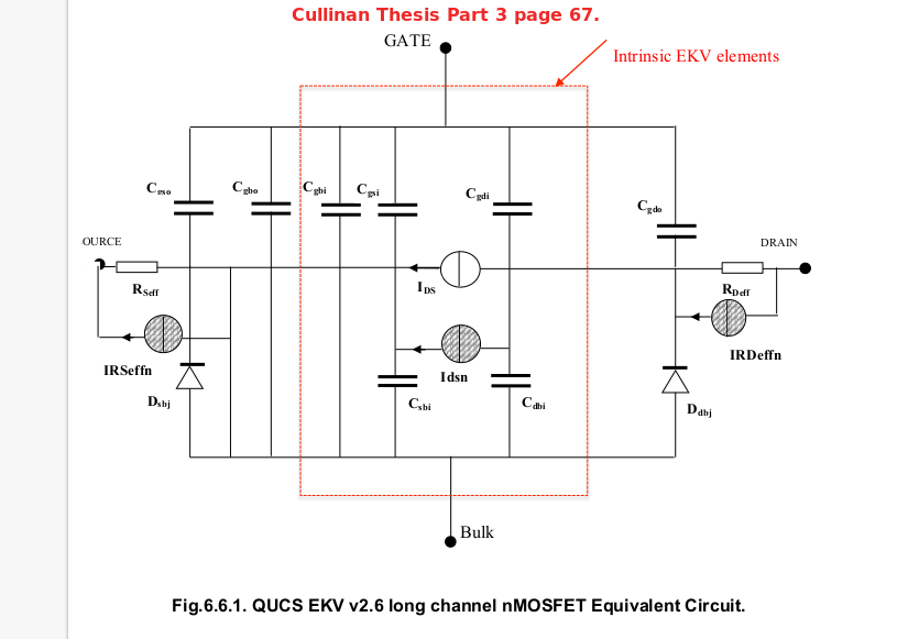
Ibid. In Part 3 page 67 Cullinan begins to made direct reference to modeling the EKV v26 Long Channel nMOSFET device as an equivalent circuirt and a QUCS entity. This divergence between Part 2 and Part 5 provides background needed to understand the schematic/symbol, Equation Defined Devics, subcircuits, transient mode operation, and test congifurations used for simulation. |
| No Image Used | Cullinan Thesis Part 5 plus supporting Abbottanp work product |
|
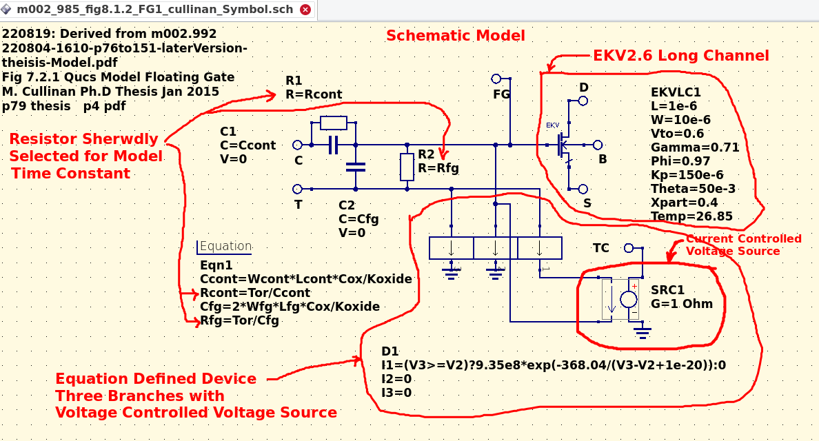
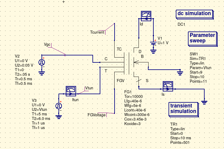
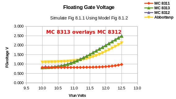
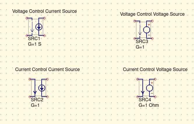
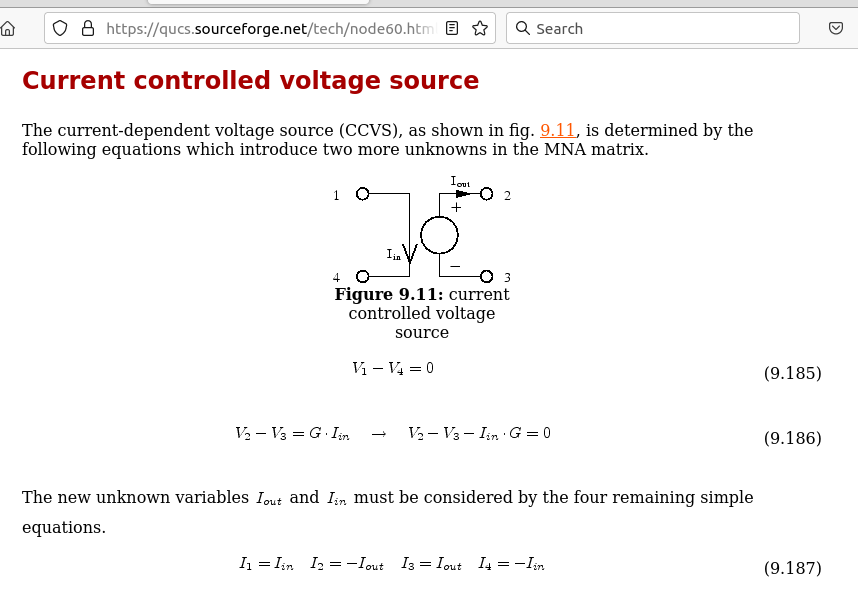
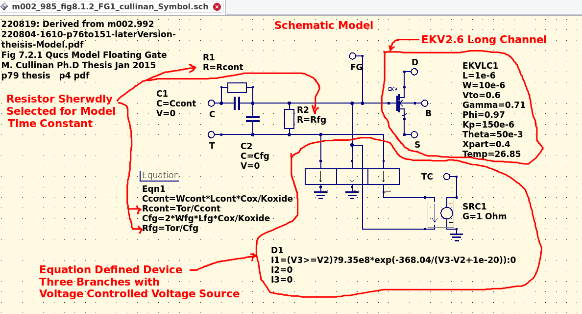
Ibid. Part 5 Page 89 displays Fig 8.1.2 Schematic subcircuit for Floating Gate transisitor, FG1. This schematic presents the QUCS model that Cullinan's Thesis derived from his earleir discussion. It incorporates the EKV26 long channel nMOSFET, the Current Controlled Voltage Source (SRC), Equation Defined Device, as well shrewd usage of time constant resistors. The model graphically shows the 'play of the Fowler-Nordheim equations/constants' with the physical features of the device's width and length. |
Schematic With Results
Abbottanp 221029 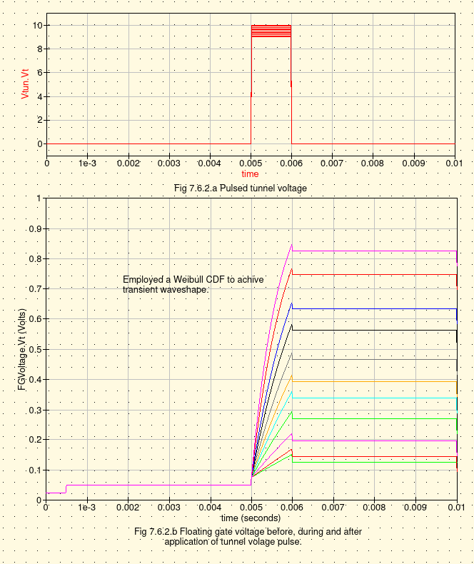
|
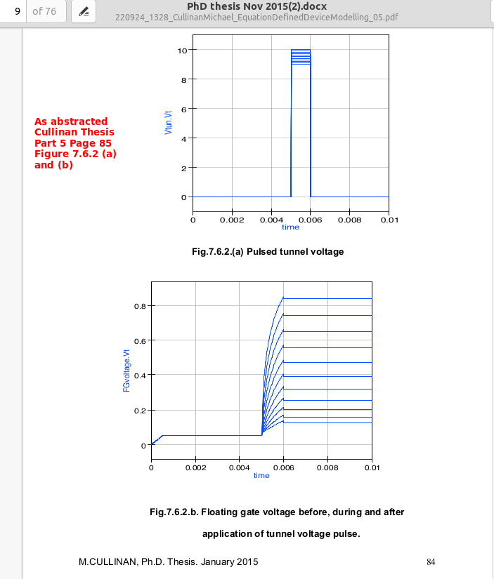
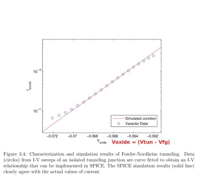
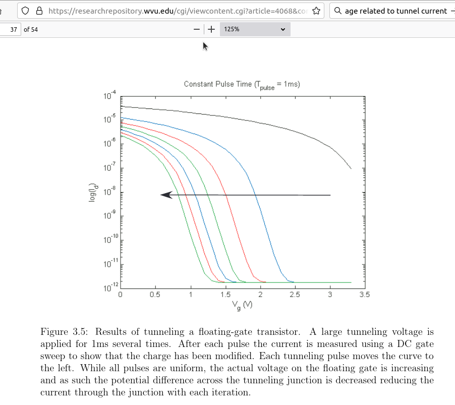
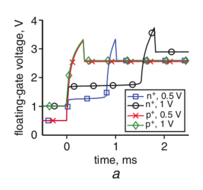
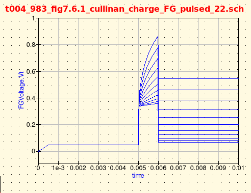
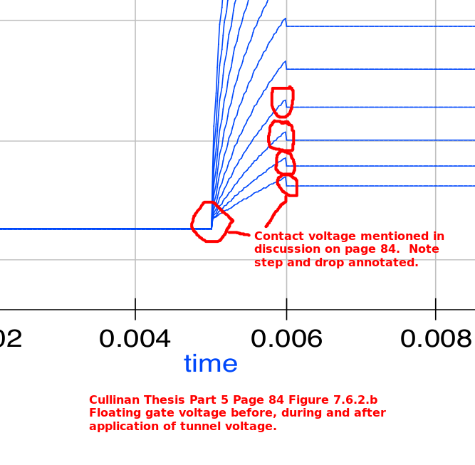
Ibid. Part 5 page 83-85 Fig 7.6.1, Fig 7.6.2 (a) & (b). The final verification of the schematic, model, and simulation test-beds
involved charging the floating gate resulting from pulsed voltages applied at the tunneling port. The simulation
results did not mirroed those found in the thesis. Discussion is provided in Issue#1 addressing this anomaly.
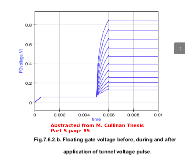
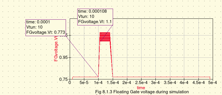
See Issue#1 to Consider The expected Floating Gate Voltage profile eluded the qucs simulation of Fig 7.6.2(b). |
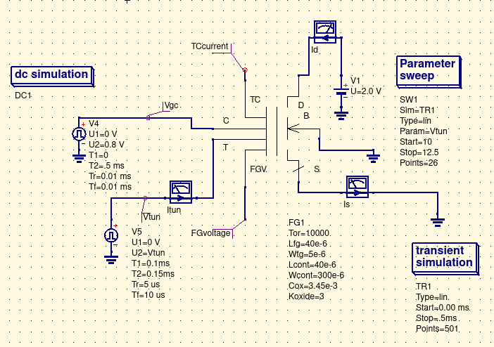
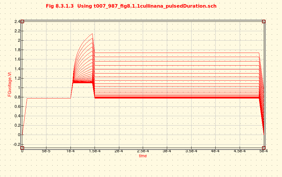
Cullinan Thesis-----Abbottanp Setup as Fig 8.3.1.3 and Fig 8.1.1 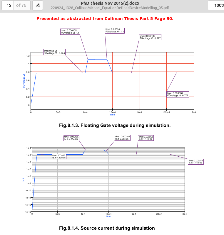
Abbottanp Recalibrate using V1 = .075 V 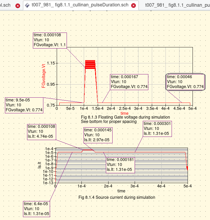
|
Ibid. Part 5 page 87- 99 Fig 8.1.1, Fig 8.1.2 plus plots labled Fig 8.3.1.1 - 8.3.1.8. The battery of simulations was replicated
with 'close' appoximation with the results shown in the thesis. Predicated upon the acceptance of the thesis the presenteed
simulation results was accpeted as 'true' for the technoogy and pulse profile specified.
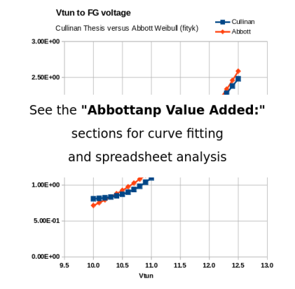
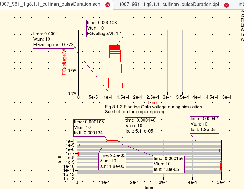
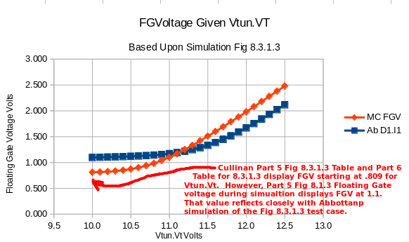
See Issue#1 to Consider The expected Floating Gate Voltage profile eluded the qucs simulation of Fig 8.1.1.1. Abbottanp simulation results for Vfg were not as expected for resulting Figure 8.3.1.1..8.3.1.3. But Figures 8.1.3 and Figure 8.1.4 matched before any best-fit fityk activity was attempted. To accommodate the 'delta' difference between the Cullinan thesis' data and Abbottanp project's rendering of the simulations, the 'fityk' curve fitting of the Cullinan thesis data was aaumed to be adequate representation of the Floating Gate Voltage (FGvoltage.Vt). With this assumption further work continued to develop a 'workable feel' for a single cell of the Floating Gate Electron Reservoir Power Source as represented as the test-bed and model presented in Fig 8.1.1 and Fig 8.1.2. Series 2 through Series 4 (Part 5 pages 100-125 remain to be processed/studied. These three series represent special case await investigation as time permits. The three series represent lesser order significance to this project. |
| Abbottanp Value Added: Curve fitting using fityk submitting Cullinan simulation data for salient test runs. Resulting best fit curves/equations used for FGV, Itun, and Is.It analysis to acquire basic cell ideal charge capacity. | |
|
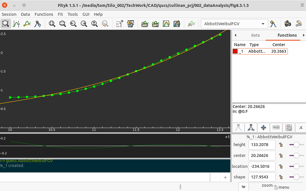
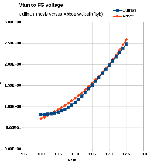
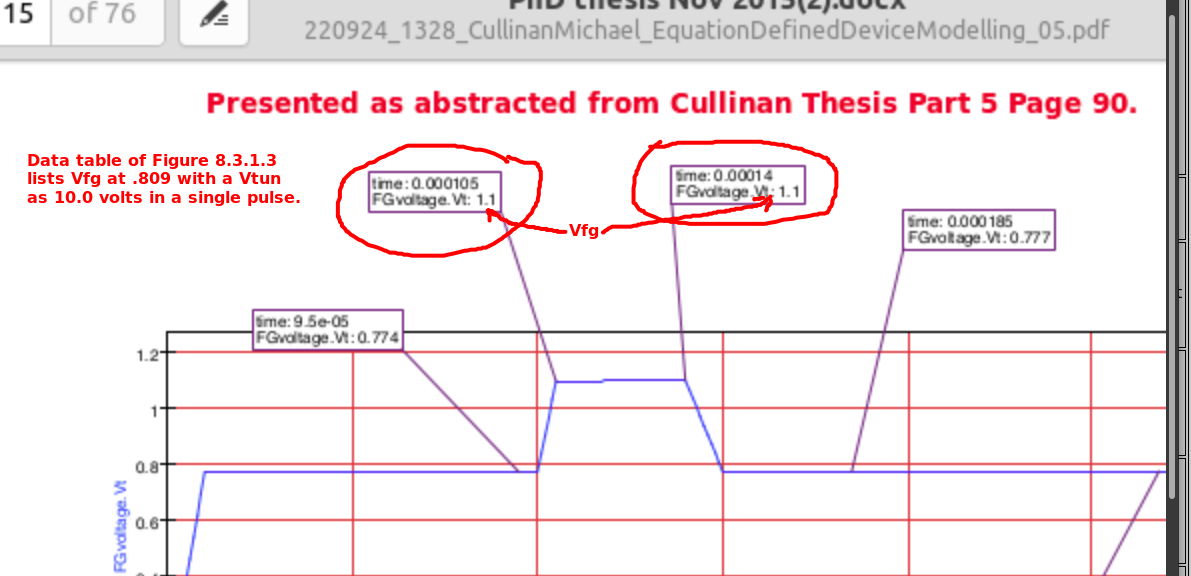
8.3.1.3 Floating Gave Voltage after pulse fall: Curve fitting via fityk yielded equation:
Given Itun A = (x > 9.9999 and x < 12.5001) define AbbottWeibulFGV(height=133.2078, center=20.26626, location=-234.5016, shape=127.9543) = height * (1-exp(-( (x-location) / (center-location) )^shape) ) |
|
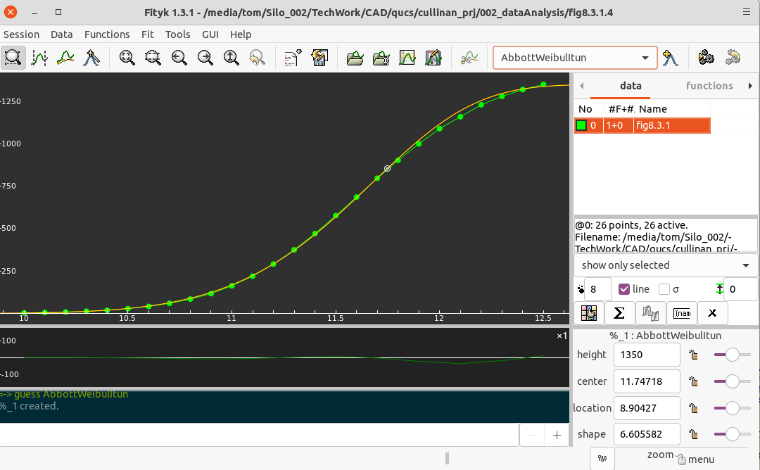
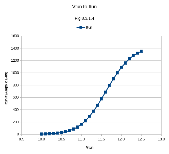
8.3.1.4 Itun during pluse: Curve fitting via fityk yielded equation:
Given Itun A = (x > 9.9999 and x < 12.5001) define AbbottWeibulItun(height= 1350, center= 11.74718, location= 8.90427, shape=6.605582) = height * (1-exp(-( (x-location) / (center-location) )^shape) ) |
|
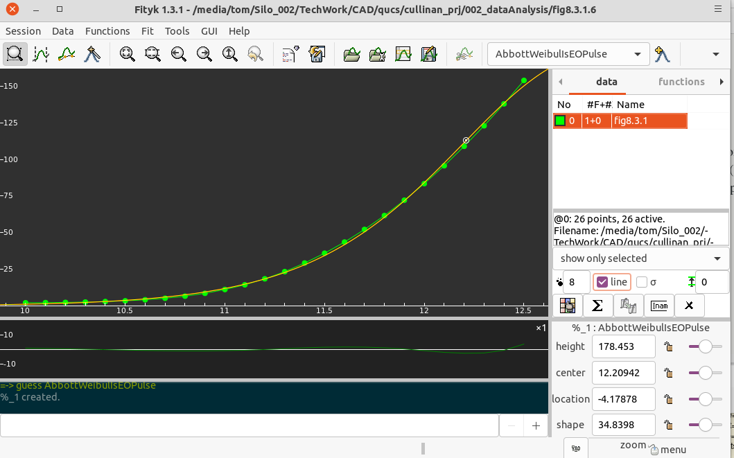
8.3.1.6 Is at end of pulse before fall: Curve fitting via fityk yielded equation:
Given FGvoltage A = (x > .8 and x < 2.5) define AbbottWeibulIsEOPulse(height= 178.453, center= 12.20942, location= -4.17878, shape=34.8398) = height * (1-exp(-( (x-location) / (center-location) )^shape) ) |
|
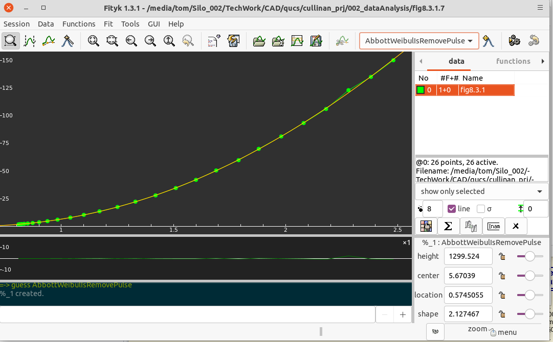
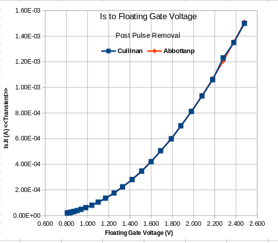
8.3.1.7 Is after pulse removed: Curve fitting via fityk yielded equation:
Given FGvoltage A = (x > .8 and x < 2.5) define AbbottWeibulIsRemovePulse(height=1299.524, center=5.67039, location=0.5745055, shape=2.127467) = height * (1-exp(-( (x-location) / (center-location) )^shape) ) |
| Abbottanp Value Added: Two separate collections of spreadsheets were produced from the data collected running Fig 8.1.1 and Fig8.1.2 (Abbottanp: m002_985_fig8.1.2_FG1_cullinan_Symbol.sch and t007_981_ fig8.1.1_cullinan_pulseDuration.sch) The data collected (data: t007_981_ fig8.1.1_cullinan_pulseDuration.dat and display: t007_981_ fig8.1.1_cullinan_pulseDuration.dpl) were directly submitted to analysis using spreadsheet 221106_1356_m002_t007_981_wargaming.ods. | |
|
File: 221107_*wargaming.ods
Sheet: m002_985_analysis 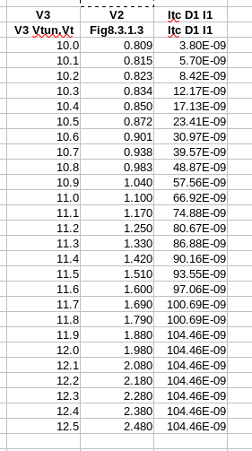
|
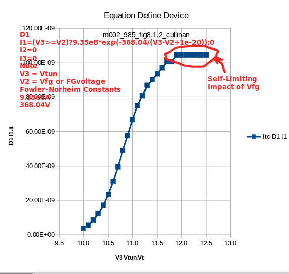
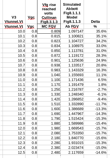
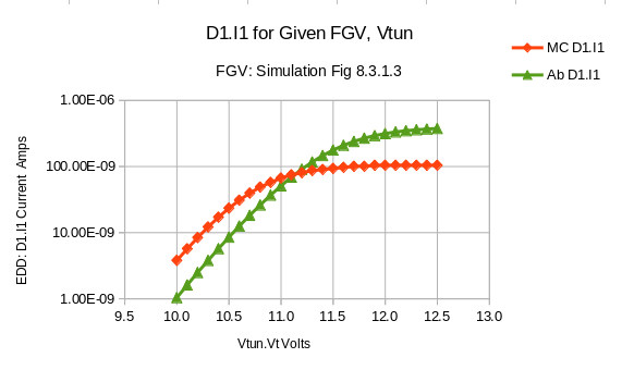
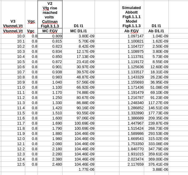
Standalone Analysis m002_985_fig8.1.2_FG1_cullinan_Symbol.sch: A spreadsheet analysis was performed using the EDD (Equation Defined Device) model supporting Fig8.1.1 simualtion testing. The spreadsheet analysis of that data plotted and graphed yielded pawned from the independent variable Vtun.Vt range (10 to 12.5 volts incremented a .1 of a volt) submitted to the Fowler-Nordheim equation as shown in the m002_985_fig8.1.2_FG1_cullinan_Symbol.sch shematic briefly discussed earlier in the Cullinan Thesis. |
|
File: 221107_*wargaming.ods
Sheet: Chap8_AbbottWeibull_FGV 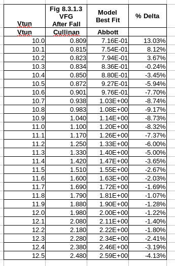
|
8.3.1.3 Floating Gate Voltage after pulse fall: Spreadsheet analysis provided confidence that the Cullinan data and AbbottWeibulFGV
model/equantion where very close appoximations. The 'slope' parameter 127.9543 caused 'floating point' issues with the
spreadsheet analysis application. The value 127.0000 usage result in no 'floating point' issue. But it did result in a marginally
higher FGV in numerous instances.
See Issue#1 to Consider The expected Floating Gate Voltage profile eluded the qucs simulation of Figure 8.1.1.1 schematic resulting in Figure 8.3.1.3 table of data. |
|
File: 221107_*wargaming.ods
Sheet: Chap8_AbbottWeibull_Itun 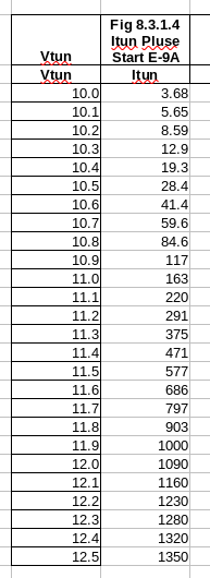
|
8.3.1.4 Tunnel Voltage to Itun at start of pulse: A spreadhsheet analysis was not pefromed since the fityk curve fitting of the Cullinan thesis showed a very 'tight' fit. This curve was not anticipated to be requred for the next level of analysis. |
|
File: 221107_*wargaming.ods
Sheet: Chap8_AbbottWeibull_Is 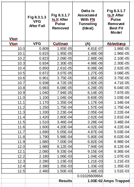
|
8.3.1.7 Is after pulse removed: This is the money-shot''. As such a deeper spreadsheet analysis was performed.
First subset analysis, the delta between Is.It DC/Steady-State and the Transient mode was determined for for each Floating Gate voltage (between .8 and 2.5). The 'delta values were collected in a 'bucket' and a summed. The resulting value was 1.03E-2 Amps trapped in the Flaoting Gate. The conversion task to Charge was planned to be performed in a separate analysis which follows shortly. The results sugest the current that can be trapped within a Floating Gate Electron Reservoir Power Source basic cell. Due the cirticality of this set of spreadsheet analysis, the second subset analysis was requred to demonstrate that the fityk best fit curve closely reflects the Cullinan test data. The correcponding plot clearly show a very, very tight fit. |
|
File: 221107_*_stateMachine.ods
Sheet: Calculate 
|
Standalone Analysis Using Chap8_AbbottWeibull_Is Results: Assuming that the Cullinan-Abbottanp analysis stands peer-review, the results: charge can be trapped within a Floating Gate Electron Reservoir Power Source basic cell is converted to Charge expressed as electron-volts. The number of basic cells required to build an 80KWHr loating Gate Electron Reservoir Power Source entity was calculated and displayed in the spreadsheet analysis. No assumption was made at this point about technology feasibility, power supply efficiency, reliability, etc. |
| TBD |